TDM Technology

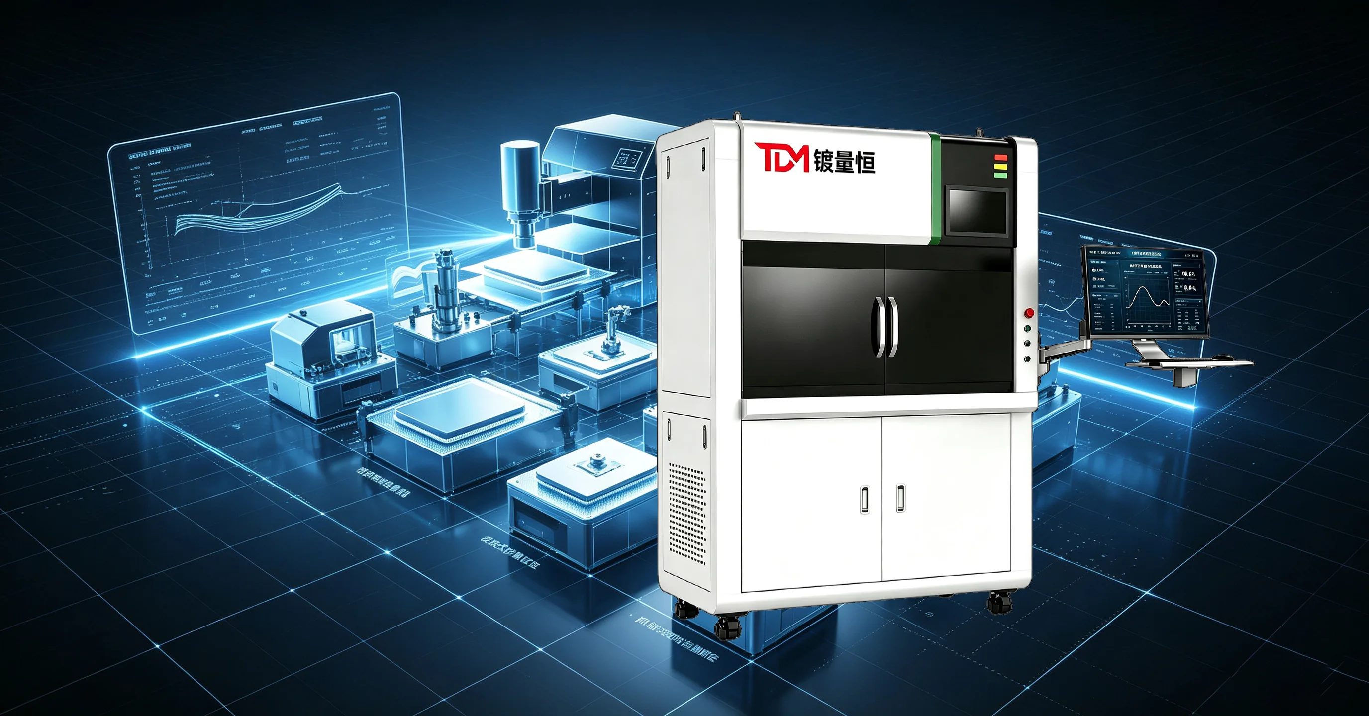
High-Precision Thin Film Measurement Equipment for Semiconductor, PV & Display

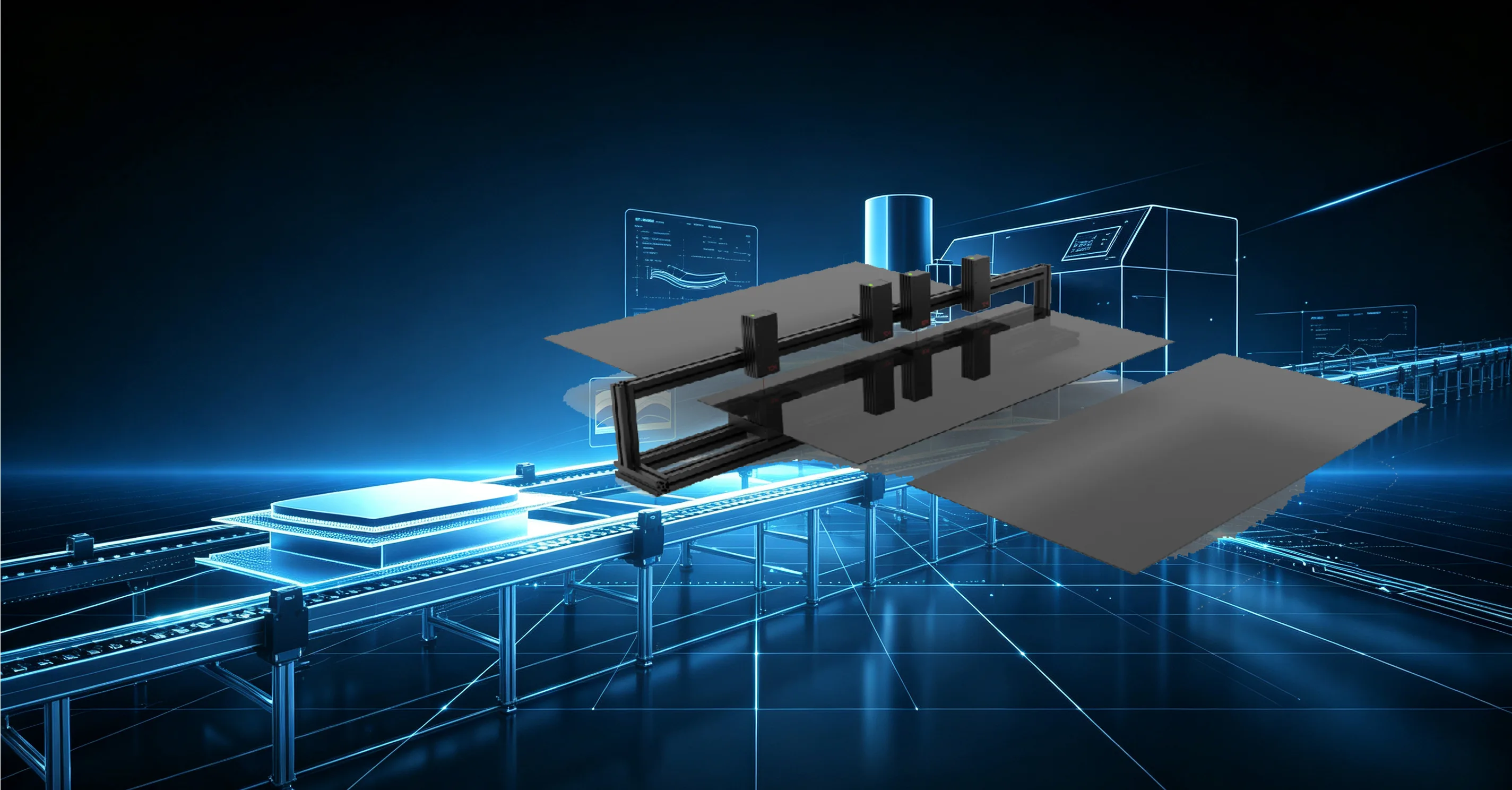
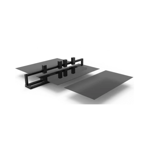
In-situ real-time coating monitoring on a PV production line

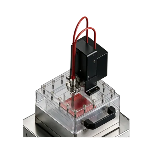
In-situ Real-time Coating Monitoring for PV Production Lines

In-situ closed-loop control for perovskite and coated battery cell production processes

In-situ Equipment

About TDM · Professional R&D Team

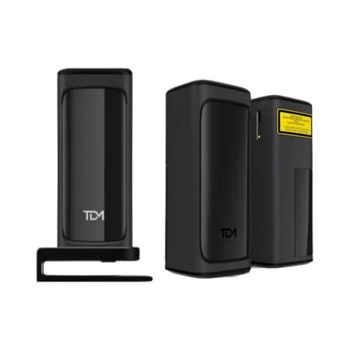
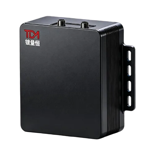
Founded in 2023, TDM Technology is headquartered in Suzhou, China, with a Shenzhen branch. Regional partners support marketing and after-sales in the US, Germany, the UK and Japan. We specialize in high-precision thin film measurement equipment for semiconductor, PV and display manufacturing. Guided by first-principles thinking, we develop optical metrology, PL/AOI and 3D profiling systems. Published products provide model-specific combinations of thickness, reflectance, transmittance, n/k, band gap, PL and mapping across offline, inline and in-situ configurations. SE31 and SE310 monitor film thickness and reflectance from the coating head. SE31-FM provides a separate wide-band transmission/reflection optical-film monitoring route; specifications are model-specific.

Core R&D Team: Composed of senior physicists and optical engineers with backgrounds from CAS and overseas labs. The core R&D team has 20+ years of experience, covering the full spectrum from material R&D and prototyping to mass production deployment.

Leveraging deep expertise in physics and optics, TDM delivers stable, high-precision, closed-loop measurement solutions for the new energy, semiconductor, and display industries. We drive technological innovation to enhance quality, yield, and intelligent manufacturing for our partners.

TDM Technology campus
10+
Self-owned Patents
2023
Year Founded
50%
R&D Personnel
50+
Partner Organizations
ISO 9001
ISO 14001

Core Advantages

Full Scenario Coverage

Covers offline laboratory equipment, inline production line integration, and two in-situ monitoring routes for active coating processes. SE31 and SE310 monitor film thickness and reflectance from the coating head. SE31-FM provides a separate wide-band transmission/reflection optical-film monitoring route; specifications are model-specific. Explore the in-situ film thickness monitoring platforms and control interfaces.

Multi-Industry Adaptability

Versatile for PV, semiconductor, display panels, optical coatings and new energy. Supports multi-layer composite films, metal/dielectric/ITO layer detection, and thin film characterization across industries with validated process recipes.

Self-Developed Core Technology

Published systems cover optical film thickness, reflectance, transmittance, n/k, band gap, PL, mapping and 3D profiling. Measurement range, repeatability, spot size and sampling mode are specified by model rather than shared across every platform.

One-Stop Service

Complete support from equipment supply and production line integration to software, on-site calibration and lifetime after-sales service. Your process engineers work directly with our application specialists from day one.

Five Major Series of Thin Film Measurement Equipment

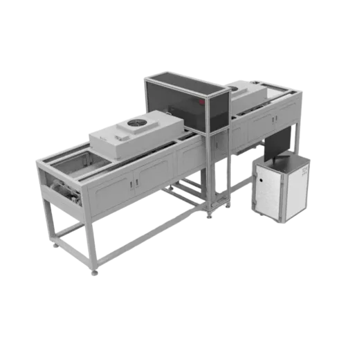
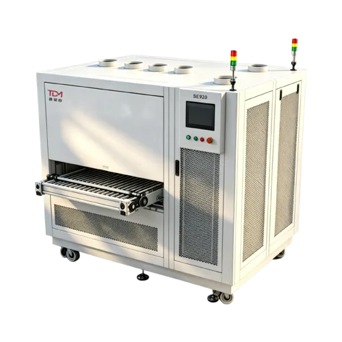
Inline thin film measurement system

Inline Production Line Measurement

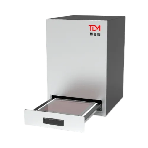
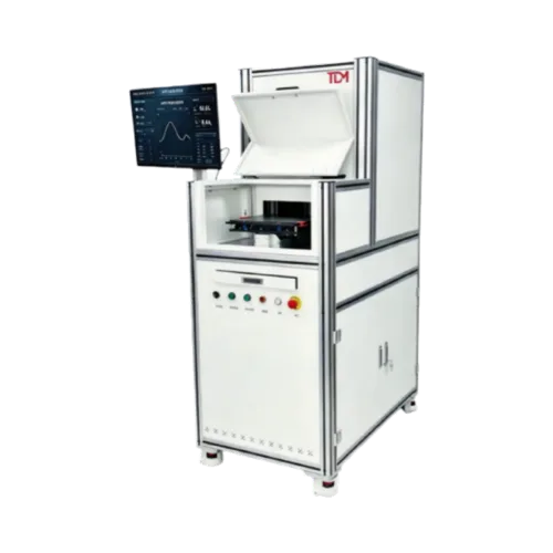
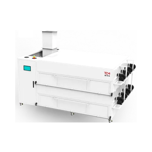
Real-time inline metrology for PV and display production lines. Monitors coating thickness and uniformity at full line speed without interrupting production, enabling immediate process feedback and higher yield. Explore inline measurement systems

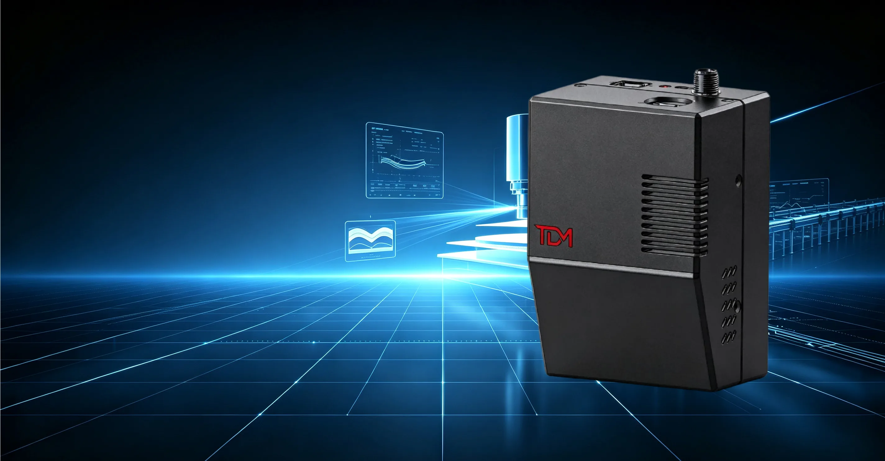
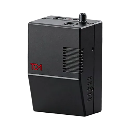
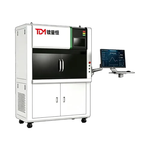
In-situ thin film measurement module

In-situ Real-time Monitoring

SE31 and SE310 monitor film thickness and reflectance from the coating head. SE31-FM provides a separate wide-band transmission/reflection optical-film monitoring route; specifications are model-specific. Compare SE31, SE310 and SE31-FM

Thin Film Measurement Equipment for Your Industry

Photovoltaic Manufacturing

Film thickness and uniformity control for PERC, TOPCon and HJT cells, plus EL/PL inspection for micro-cracks, PID and degradation analysis.

Explore PV solutions

Semiconductor Fabrication

Nanometer-level metrology for SiO₂, SiN, poly-Si and metal stacks on 200/300mm wafers — available in offline and inline configurations.

Explore semiconductor solutions

Display & Panel Production

Thickness and optical property monitoring of ITO, organic layers and barrier films for OLED and microLED manufacturing lines.

Explore display solutions

Optical Coatings & New Materials

Precision control of AR/HR coatings, filters and beam splitters, with thin film characterization support for R&D and pilot production.

Explore optics solutions

R&D and Technical Strength

  • 10+ self-owned thin film measurement patents
  • 50% of personnel work in R&D
  • Core R&D team with 20+ years of experience
  • Offline, inline and in-situ product configurations
R&D and production line

Customer Feedback on Thin Film Measurement

Illustrative feedback from semiconductor, PV, display and optical coating applications. These notes describe typical use of TDM thin film measurement equipment for thickness, uniformity and inline inspection. They are not attributed to named individuals or verified customer accounts.

Feedback from a semiconductor manufacturer

Semiconductor manufacturer

Cost and functionality are well balanced for our thin film measurement needs. We plan to expand the same configuration across more production lines.

Feedback from a PV manufacturer

PV manufacturer

On our PV pilot line, film thickness and defect maps have stayed consistent from shift to shift after deploying defect mapping inspection.

Feedback from a PV production team

PV manufacturer

We needed cost-effective inspection to replace an aging lab setup. SE20 now covers most thin-film detection work on the production floor.

Feedback from an optical coating manufacturer

Optical coating manufacturer

Measurement accuracy met our coating-line requirements. Integration was smooth, and application support stayed responsive.

Feedback from a display manufacturer

Display manufacturer

Inline inspection reduced scrap. Operators can read coating thickness without slowing the line.

Feedback from a semiconductor process team

Semiconductor manufacturer

From sample testing to on-site commissioning, the metrology setup matched our production requirements.

Frequently Asked Questions About Thin Film Measurement

How is thin film thickness measured?

Thin film thickness is measured with optical and imaging configurations matched to the film stack, substrate and required output. TDM thin film measurement equipment covers published offline, inline and in-situ configurations. Selection depends on thickness range, sample size, spot size and whether thickness, T/R, n/k, PL or mapping is required. See film thickness measurement solutions.

What is the difference between inline and in-situ measurement?

Inline measurement is performed at a defined point in the production flow, typically after a process step or between process steps. In-situ measurement monitors the film at the active coating process. TDM provides coating-head wet-film thickness and reflectance monitoring with SE31/SE310, plus wide-band transmission/reflection optical-film monitoring with SE31-FM. Explore in-situ metrology solutions.

Can thin film measurement be done without contact?

Yes. Selected TDM thin film measurement equipment supports non-contact measurement; for example, SE200 publishes non-contact micro-area detection through a microscope C-mount interface. Suitability depends on the material system, surface condition, film structure and measurement objective. Explore non-destructive thin film metrology systems from TDM.

How do you detect PV module defects?

PV module defects can be evaluated using applicable electrical, imaging, environmental and mechanical test methods. Electroluminescence imaging can help identify selected defects, including micro-cracks, broken fingers and potential-induced degradation indicators, while IV curve testing evaluates electrical performance. The appropriate test plan depends on the module type, production stage and evaluation objective. Explore PV reliability and electrical safety testing systems and PV electroluminescence testing.

View All Thin Film Measurement FAQs

Get a Technical Consultation

Tell us your film stack, substrate and production environment — our application engineers will recommend the right thin film measurement equipment configuration.

  • Free on-site production line survey
  • Free sample testing experiments
  • Customized equipment scheme design